
What You Need to Know About BGA Soldering
Ball Grid Array (BGA) soldering is one of the most crucial techniques in modern electronics manufacturing, especially for high-density printed circuit boards (PCBs). As devices get smaller yet more powerful, BGA packages have become the preferred choice for mounting integrated circuits (ICs) like processors, FPGAs, and memory modules. However, BGA soldering demands precision, skill, and proper equipment to ensure reliable electrical and mechanical connections.
This article provides a complete overview of what BGA soldering is, its process, challenges, advantages, inspection techniques, and key best practices every electronics professional should know.
Introduction: What is BGA Soldering?
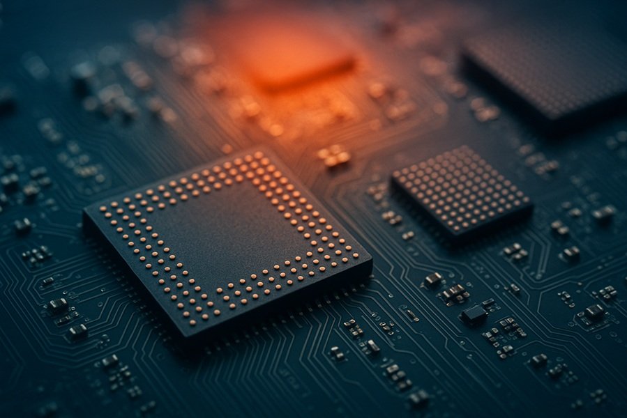
BGA (Ball Grid Array) is a surface-mount packaging method used to permanently mount devices such as microprocessors onto PCBs. Unlike traditional pin-based packages, BGA components use solder balls arranged in a grid on the underside of the chip. These solder balls serve as both the electrical connections and the physical mounting points.
BGA soldering is the process of attaching these packages to the PCB using reflow soldering, where solder balls melt and bond to copper pads on the board during controlled heating.
Read This: Understanding PCB Warpage: Causes, Effects, Standards & Solutions
Why Use BGA Packages?
BGA packages became popular as traditional leaded packages (like QFP and DIP) reached their limits in terms of pin density and electrical performance.
Key reasons for using BGA packages include:
- Higher I/O density: BGAs can house hundreds to thousands of connections in a compact form.
- Better electrical performance: Shorter connections reduce inductance and resistance.
- Enhanced thermal performance: Heat dissipates through the solder balls and package body.
- Reduced size and weight: Ideal for modern compact devices like smartphones and laptops.
Components of a BGA Package
A typical BGA package includes the following:
- Silicon Die: The core semiconductor chip.
- Substrate: Provides routing between the die and solder balls.
- Solder Balls: Small spheres of solder that make contact with the PCB pads.
- Encapsulation: Protective layer covering the die and interconnections.
BGA Soldering Process: Step-by-Step
BGA soldering typically involves automated assembly lines, but the process principles remain the same even in manual rework.
1. PCB Preparation
- Clean and inspect the PCB pads to ensure no contamination or oxidation.
- Apply solder paste using a stencil printer for consistent deposition.
2. Component Placement
- A pick-and-place machine precisely positions the BGA on the PCB.
- Proper alignment is essential to ensure each solder ball sits correctly on its pad.
3. Reflow Soldering
- The assembly enters a reflow oven where it undergoes a controlled thermal profile:
- Preheat stage: Gradually warms the PCB to prevent thermal shock.
- Soak stage: Activates the flux and removes oxidation.
- Reflow stage: Raises temperature above solder’s melting point (~220°C).
- Cooling stage: Solidifies the solder joints.
4. Cleaning and Inspection
- After reflow, flux residues are removed if necessary.
- X-ray inspection is performed to verify hidden solder joints.
Reballing: Repair and Rework Process
Sometimes, BGA components need to be removed and replaced — a process known as reballing.
Steps in BGA Reballing:
- Desoldering: Use a rework station to heat and remove the BGA chip.
- Cleaning: Remove residual solder from both the board and the chip.
- Reballing: Apply a stencil and deposit new solder balls on the BGA pads.
- Placement & Reflow: Realign the BGA and solder it back using a reflow process.
Reballing is commonly used in repair centers and prototyping to fix defective joints or reuse expensive chips like GPUs.
Common Challenges in BGA Soldering
BGA soldering, though efficient, comes with its share of technical challenges:
| Issue | Description | Possible Cause |
|---|---|---|
| Cold solder joints | Incomplete melting of solder | Improper reflow temperature |
| Bridging | Adjacent solder balls connect | Excess solder paste or misalignment |
| Open circuits | Missing solder connections | Poor wetting or misalignment |
| Voids | Air pockets within solder joints | Rapid heating or trapped flux gases |
| Component warpage | BGA lifts during reflow | Uneven temperature or mechanical stress |
BGA Soldering Inspection Techniques
Since BGA joints are hidden beneath the component, visual inspection is impossible. Engineers rely on advanced tools to ensure connection integrity.
1. X-Ray Inspection
- Non-destructive and most widely used method.
- Detects bridging, opens, voids, and misalignment.
2. Automated Optical Inspection (AOI)
- Useful before and after reflow (for alignment check).
- Cannot see under the BGA body but identifies placement issues.
3. Cross-Sectional Analysis
- Destructive testing method to study solder joint microstructure.
- Used in quality control and failure analysis.
Best Practices for Reliable BGA Soldering
- Use a proper reflow profile – Follow manufacturer-recommended temperature settings.
- Maintain clean surfaces – Remove oxidation and residues for better wetting.
- Ensure correct stencil design – Proper aperture size ensures even solder distribution.
- Avoid moisture absorption – Store BGA packages in dry conditions (use desiccants).
- Use X-ray verification – Always inspect solder joints in critical assemblies.
- Control rework cycles – Excessive heating can damage the component or PCB.
Equipment Used in BGA Soldering and Rework
- Reflow Oven: For bulk soldering of BGA components.
- BGA Rework Station: For precise heating, removal, and reballing.
- Hot Air Gun / Infrared Heater: For localized heating.
- Stencil Printer: For accurate solder paste deposition.
- X-Ray Inspection System: For non-destructive joint verification.
Advantages of BGA Soldering
- High electrical and thermal performance
- Compact footprint for modern electronics
- Stronger mechanical bond compared to fine-pitch leads
- Lower signal distortion and noise
- Enhanced reliability for high-speed circuits
Applications of BGA Packages
BGA soldering is extensively used in high-performance and compact electronics, such as:
- Smartphones and tablets
- Laptops and motherboards
- Game consoles
- Automotive control units
- Aerospace and defense electronics
- Industrial embedded systems
Future of BGA Soldering
With the growing demand for miniaturization and power efficiency, BGA technology continues to evolve. Advanced forms like CSP (Chip Scale Package), Micro-BGA, and PoP (Package on Package) are being developed to pack more functionality into smaller footprints.
Emerging trends like lead-free soldering, AI-driven inspection systems, and automated rework robotics are making BGA assembly more reliable and eco-friendly.
Conclusion
BGA soldering is a cornerstone of modern PCB manufacturing, enabling compact, high-performance electronics. However, it requires precise process control, specialized equipment, and thorough inspection to ensure success.
For engineers and technicians, mastering BGA soldering means combining technical understanding, attention to detail, and familiarity with inspection tools — all of which are crucial for producing reliable, next-generation electronic devices.


