
7 Factors for Selecting a Singapore PCB Partner for Advanced Photonics and Power Electronics
The global electronics landscape is currently witnessing a paradigm shift. As Artificial Intelligence (AI) infrastructure, electric vehicles (EVs), and high-speed telecommunications converge, the demand for Printed Circuit Boards (PCBs) has evolved from simple component carriers to complex, high-performance thermal and optical management systems. In Singapore, a global hub for semiconductor excellence, the stakes are particularly high.
For industries dealing with advanced photonics and power electronics, the standard “quick-turn” prototype shop is no longer sufficient. These sectors require specialized materials, extreme thermal management, and sub-micron precision. At Gennex, we understand that selecting a manufacturing partner is not merely a procurement decision—it is a strategic engineering partnership.
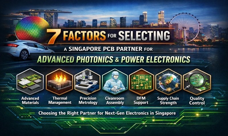
If your organization is scaling advanced electronic systems, here are the seven critical factors you must evaluate when vetting pcb manufacturing companies in singapore.
1. Mastery of Advanced Substrates and Material Science
Power electronics, especially those utilizing Silicon Carbide (SiC) and Gallium Nitride (GaN), operate at much higher temperatures and frequencies than traditional silicon-based components. Consequently, standard FR4 substrates are often inadequate.
A Tier-1 partner must demonstrate expertise in:
- Metal Core PCBs (MCPCBs): Essential for heat dissipation in high-power LED and automotive applications.
- Ceramic Substrates: Offering superior thermal conductivity and electrical isolation for power modules.
- High-Frequency Laminates: Critical for photonics and 6G telecommunications to minimize signal loss.
2. Thermal Management and Heavy Copper Capabilities
In power electronics, heat is the enemy of reliability. Selecting a partner that can handle “Heavy Copper” (3oz to 10oz or more) is vital for carrying high currents without excessive temperature rises. Furthermore, look for advanced thermal via technologies, such as copper-filled vias or sophisticated heat sink integrations, which allow heat to be pulled away from sensitive photonics components efficiently.
3. Precision Metrology and Quality Control
In the world of photonics, a misalignment of a few microns can render an entire board useless. This is where the laboratory environment of your PCB partner becomes a deciding factor. An authoritative partner invests heavily in high-end measuring laboratory equipment to verify impedance, trace geometry, and surface roughness.
You should inquire about their use of:
- Coordinate Measuring Machines (CMM): For dimensional accuracy.
- X-Ray Fluorescence (XRF): To verify plating thickness and RoHS compliance.
- Scanning Electron Microscopy (SEM): For failure analysis and sub-surface inspection.
4. Cleanliness Standards and Chemical Compatibility
Advanced electronics are highly sensitive to ionic contamination. Leftover flux residues can lead to electrochemical migration and dendrite growth, eventually causing short circuits. This is particularly dangerous in high-voltage power electronics.
A high-quality partner must have a rigorous cleaning protocol. With the industry-wide shift away from legacy solvents, it is crucial to ensure they utilize modern, high-performance fluids like novec flux remover or its qualified 2026-compliant alternatives. These fluids provide the low surface tension required to penetrate under tight-pitch components (like BGAs and QFNs) to ensure the board is chemically pristine before conformal coating or final assembly.
5. Specialized Assembly for Photonics (Active Alignment)
Photonics assembly differs from standard SMT (Surface Mount Technology) because it often requires “Active Alignment.” This involves powering up the device during the assembly process to ensure that laser diodes, optical fibers, and sensors are perfectly aligned to maximize light transmission. Your Singapore partner should possess the cleanroom facilities (Class 100 or Class 1000) and the specialized pick-and-place robotics capable of handling these delicate optical components.
6. Design for Manufacturing (DFM) Support
The transition from a prototype to mass production is where most engineering projects fail. A strategic PCB partner in Singapore should provide proactive DFM feedback. This includes:
- Stack-up Optimization: Balancing signal integrity with manufacturing cost.
- Panelization Strategy: Maximizing material yield.
- Solder Mask Precision: Ensuring high-voltage clearance (creepage and clearance distances) are maintained to prevent arcing in power modules.
7. Supply Chain Resilience and Ecosystem Integration
Finally, consider where your partner sits within the Singapore semiconductor ecosystem. Singapore’s strengths lie in its integrated supply chain. A partner that has direct relationships with local testing labs, component distributors, and specialized chemical suppliers can mitigate the risks of global logistics disruptions.
At Gennex, we advocate for a “local-first” engineering approach where the proximity of the PCB fabrication to the assembly and testing site reduces lead times and allows for rapid iterative cycles—essential for the fast-moving photonics market.
Conclusion: The Gennex Standard of Excellence
Selecting a PCB partner for power electronics and photonics is a decision that impacts the entire lifecycle of your product, from MTBF (Mean Time Between Failure) to overall system efficiency. By focusing on material science, precision metrology, and rigorous cleaning standards, you ensure that your high-tech innovations are built on a foundation of reliability.
In the complex world of advanced electronics, don’t settle for a vendor. Seek a partner that understands the physics of your components as well as you do.


