
PCB Positive and Negative Difference: From Design to Process
Printed Circuit Boards (PCBs) form the core of all electronic circuits. While most discussions focus on types (single-layer, multi-layer, etc.), there is a less-known but crucial distinction during the manufacturing and design phase — positive vs. negative PCBs. Understanding this difference is vital for PCB designers, fabricators, and electronics engineers.
In this article, we’ll explore the positive and negative PCB concept, explain their differences, and cover their applications, design strategies, and manufacturing processes.
What Is a Positive PCB?
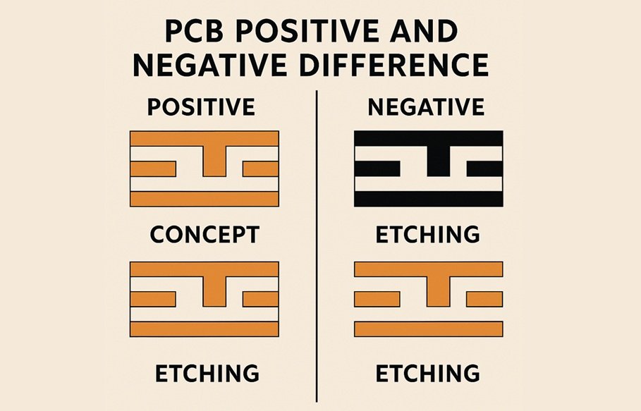
In a positive PCB, the copper areas shown in the design file are the ones that will remain after the etching process. In other words, the layout you see on the screen is a direct representation of what will appear on the final PCB.
🔍 Characteristics of Positive PCBs:
- Exposed copper traces represent actual circuit paths
- Background areas will be etched away during processing
- Design is easier to understand and visualize
- Ideal for basic and prototype boards
🛠️ Positive Process:
- Design is created in a CAD tool (like KiCad or Altium)
- Copper-clad board is coated with photoresist
- Transparent areas of the photomask allow UV light to harden the resist
- The board is developed, and non-hardened areas are washed away
- Unprotected copper is etched, leaving desired traces
Read This: Top 20 PCB Manufacturers in the World in 2025
What Is a Negative PCB?
In a negative PCB, the copper shown in the layout will be removed during the etching process. The layout represents areas to be cleared, not retained.
🔍 Characteristics of Negative PCBs:
- What you see in the file is inverted
- Black areas typically represent copper to be removed
- Used for complex, multi-layer PCBs
- Helps in controlling impedance and reducing signal distortion
🛠️ Negative Process:
- The design is created in negative format (reversed pattern)
- Opaque areas block UV light, protecting parts to be removed
- Unexposed photoresist remains soluble and is removed
- Etching clears the unwanted copper, exposing only non-black parts in the original design
Positive vs Negative PCB: Key Differences
| Aspect | Positive PCB | Negative PCB |
|---|---|---|
| Design Representation | Direct (actual traces visible) | Inverted (traces are masked) |
| Ease of Visualization | Easier for humans | Harder to read manually |
| Etching Outcome | What you see is what you get | What you see will be removed |
| Use Cases | Simple, single-layer boards | Multi-layer, complex designs |
| Manufacturing Layer | Outer layers usually positive | Inner layers often negative |
| Design Tools Required | Basic CAD | Advanced CAM capabilities |
| Common in | Prototyping, hobbyist boards | High-frequency or HDI PCBs |
Positive and Negative in PCB Layer Stacking
In a typical multi-layer PCB, outer layers (Top & Bottom) are designed as positive images, while inner layers are often done in negative format.
Example Layer Stack:
- Top Layer (Positive) – Traces and pads are directly shown
- GND Plane (Negative) – Copper fills are shown in black to be removed
- Power Plane (Negative) – Again, only non-black zones are retained
- Bottom Layer (Positive) – Like the top, it mirrors actual layout
This distinction is crucial when using CAM tools (Computer-Aided Manufacturing) to prepare Gerber files, which are sent to PCB fabrication houses.
Why Does the Difference Matter?
Choosing between positive and negative designs affects:
✅ Manufacturing Accuracy
Negative designs for internal layers provide better etching precision, especially for power and ground planes.
✅ Signal Integrity
Negative designs help create clean copper fills, minimizing EMI (Electromagnetic Interference) and enabling controlled impedance for high-speed signals.
✅ Fabrication Cost
Positive designs are cheaper and easier to prototype, while negative designs require advanced machinery and CAM processing, increasing costs.
✅ Error Reduction
Confusing positive and negative layers can lead to short circuits, signal crosstalk, or even total board failure. Correct labeling and documentation are essential.
When to Use Positive vs. Negative?
| Application | Preferred Format |
|---|---|
| Single-layer DIY board | Positive |
| Prototyping with minimal traces | Positive |
| Inner layers of multilayer PCBs | Negative |
| High-speed signal routing | Negative |
| Mass production for IoT devices | Mix of both |
| Medical/Military applications | Negative (with strict testing) |
Tools and Best Practices
- EAGLE, KiCAD, Altium Designer allow layer format customization
- Use clear file naming: e.g.,
top_copper_positive.gbr,gnd_plane_negative.gbr - Confirm polarity before sending Gerber files to your PCB manufacturer
- Review CAM previews or generate 3D views to ensure correctness
- Communicate with the fabricator to clarify any layer stack-up conventions
Read This: How HDI Impacts PCB Lead Time: A Comprehensive Guide
Final Thoughts
The positive vs. negative PCB difference might seem technical, but it plays a crucial role in manufacturing efficiency, signal quality, and cost management. Whether you’re designing a DIY circuit or a 10-layer server board, understanding this distinction can help you avoid costly mistakes and optimize performance.
If you’re working with a PCB house or uploading Gerber files, always clarify which layers are positive and which are negative, especially for ground and power planes.


