
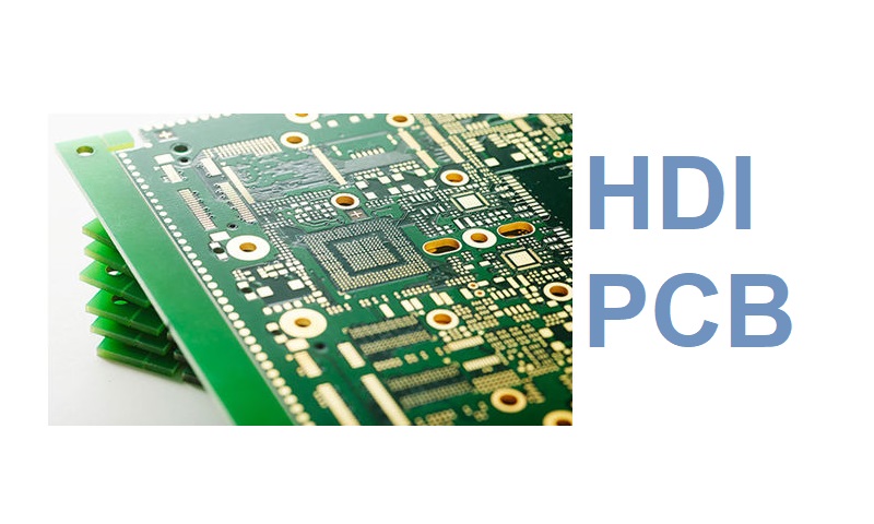
All about HDI PCB | What is HDI PCB?
PCBs or Printed Circuit Boards are vital features used by electronic products to protect electrical connections and various components in the products. The excellent news about PCBs is that wiring is not revealed. This means it is not threatening.
Nevertheless, there are different types of PCBs and various designs used to manufacture PCBs. One preliminary design is the HDI PCB.
This article will get a complete guide on what HDI PCB is, the advantages of HDI PCB, its applications, the design, and other important information you need.
What is HDI PCB?
HDI PCB or High-Density Interconnect PCB is a circuit board with better wiring than normal PCBs. It helps in reducing the electrical component’s weight and size. Also, it helps to enhance the electrical performance of the circuit board.
HDI PCBs have better accuracy and functionalities than traditional PCBs. Hence, it works better and provides better results than other PCBs.
What are the benefits of using HDI PCB?
HDI PCB has more advanced features than a traditional printed circuit board. Thus, it has many benefits over the others. Below are the main benefits of HDI PCB.
1. Less heat transfer
Due to the presence of heat on a PCB, many get damaged after a while. Happily, something can be done about the issue. One way of fixing the problem is by reducing the presence of heat.
The HDI PCB does a good task of facilitating the transfer of less heat. Moreover, the heat is made to travel further than expected before escaping from the HDI board.
2. Have an extended battery life
Unlike the traditional PCB, a High-Density Interconnector has a higher and extended battery life due to the reduced power consumption.
3. Has a consistent transmission
HDI PCB has a reliable transmission due to its compact size, which is essential when adding several components. In addition, there is more space on the circuit board.
4. Occupied sides
The sides of the HDI PCB are very populated. Due to this reason, the PCB designer and manufacturer have more space to add extra components.
5. Helps in reducing the weight of the products
The introduction of HDI PCB has helped reduce the weight of the products. Since a board is compact, it makes it easier to fit in any type of product. Moreover, it hides the wires and other components well to avoid obstruction during connection.
6. There are many HDI PCB applications
Due to its numerous benefits, HDI PCB can be used on many products and many things. Some of these applications include medical gadgets, 4th generation network communications, electronic aircraft parts, mobile devices, digital cameras, laptops, and many others.
7. Faster design and manufacture time
Another main benefit of HDI PCB is that the manufacturer can design and manufacture the boards in a short time. It provides a faster turnaround time for many reasons.
First, there is no need to relocate the board’s components constantly. Also, the SMD elements are quickly placed on the circuit board.
Applications of HDI PCB
HDI PCBs are used in various sectors. Some of the applications of HDI PCB include:
1. Healthcare
Most medical sector PCB designers are using the latest innovations. Hence, they have incorporated HDIs since they are smaller and can fit well in implants and imaging equipment.
These gadgets play a significant role in treating diseases. For instance, a heart pacemaker is a gadget attached to a human heart to maintain circadian rhythms. So, with HDI PCB, manufacturers can manage to produce smaller pacemakers that are more efficient.
2. Automotive industry
Vehicle manufacturers are using HDI PCBs because there is more innovation due to the chips. With an HDI PCB, you can save space and increase performance. Thanks to HDI PCBs, hybrid cars run their electronic functions well.
3. Digital gadgets
When you compare digital gadgets with those of ten years ago, you will notice the modern ones are lighter and smaller. This is due to the use of HDI PCB. The introduction of HDI PCB helps the manufacturer produce thinner, portable, and more effective mobile devices.
4. Military and aerospace
Missiles and various defense communication systems use HDI PCB in the military field. In addition, the aerospace sector is changing to HDI PCB to have smaller and lighter gadgets.
Tips for designing HDI PCB
1. Check the capability of the manufacturer
When designing an HDI PCB, the first tip is to check the manufacturer’s capability. This is very important when planning a new PCB.
Keep in mind that manufacturers have different capabilities. Hence, check with your manufacturer before you develop an HDI layout.
2. Track the spacing between pads and traces
Another tip to consider when designing HDI PCB is the space between pads and traces. For instance, the clearance values of the solder masks should be similar in size to trace width.
3. Do not use EPIC or staggered Vias if you do not need them
People use HDI PCB since it offers enough space for routing on the inner layer and the surface. Hence, it is good to avoid using staggered vias if you do not need them. Please do not use the extra space until it is worth it.
4. Consider having fewer layers
If you can, consider fewer layers. This is because more layers mean higher manufacturing costs and several PCB assembly steps.
Final Word
Today, the digital world is becoming smaller and more straightforward. Your smart device is getting smarter, your computer is getting lighter, and most of your electronics are getting smaller and more efficient.
It is possible to move with your laptop and keep your business running while on a flight. In addition, it is possible to do so much on your smart device. All this is possible due to the introduction of PCBs, and mostly HDI PCBs.
With HDI PCBs, the size of most products has been reduced, and the weight is manageable. In addition, the birth of HDI PCB has led to more innovations in various sectors.


