
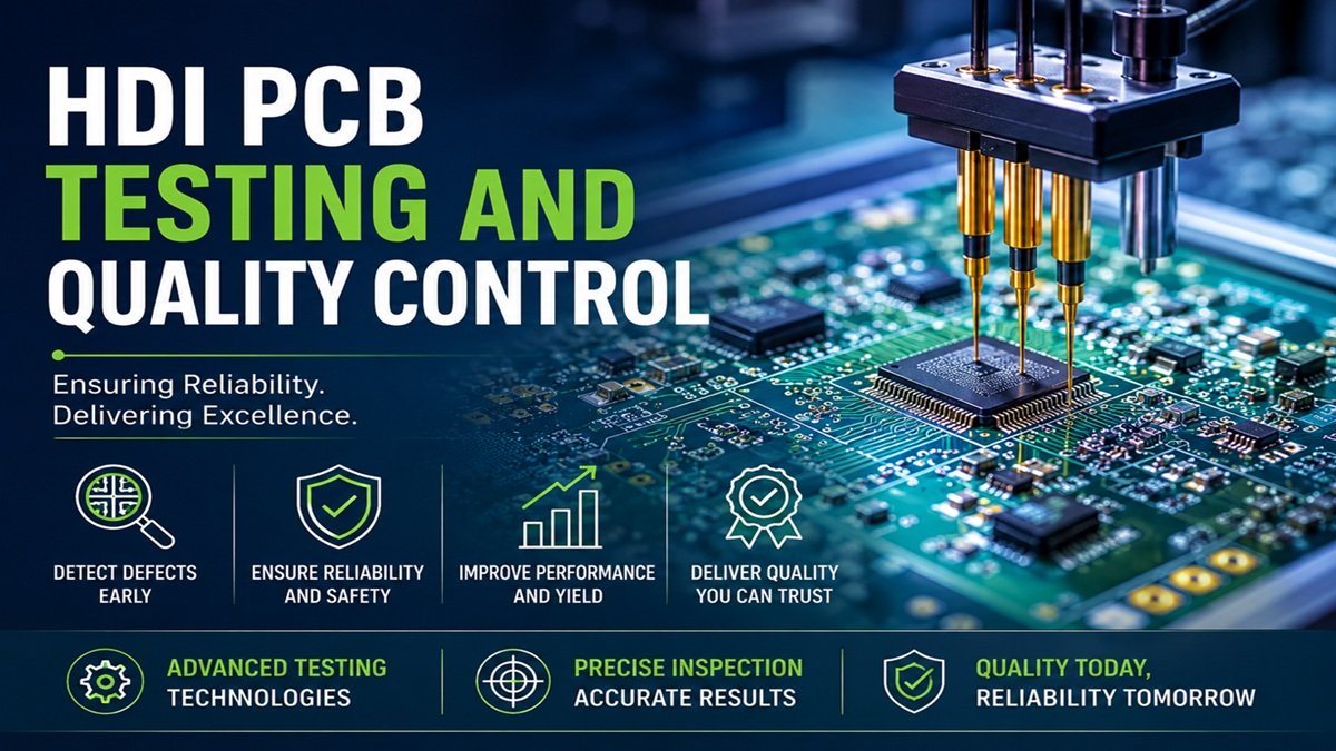
HDI PCB Testing and Quality Control
HDI PCB testing is a very important aspect in reliability. The High-Density Interconnect PCBs have a very compact and complex circuitry. These boards run today’s smartphones, medical devices and autos systems. The stakes are high on them to perform so accuracy in manufacturing and testing is a must. Even an insignificant flaw may lead to significant system malfunctions.
Quality control of PCBs can be used to identify these inside defects before they get to final consumers. Visual inspections and automated testing are only two of the means that are important. Compliance is not the only thing about testing; it is about confidence.
HDI PCB manufacturing integrates high functionality and miniaturizing. Such complexity requires stricter quality control points, and sophisticated testing procedures. In this high-tech world that is so fast-paced, quality PCBs are not negotiable. Quality control provides the manufacturers with a sense of security and the customers with reliable products.
This paper discusses the concept of HDI PCB testing, its importance and practices that yield the most desirable performance. You will discover tips, techniques, and tools that are applied in the contemporary PCB quality control systems. As an engineer or a production worker, this knowledge can assist you in minimizing mistakes and improving the level. We are going to take a look at the invisible world of testing and control.
Why Is Testing and Quality Control Critical for HDI PCBs?
HDI PCB Testing ensures every board meets strict standards. These boards are compact but packed with essential components. With such density, even minor defects can cause major disruptions. Quality control isn’t just a step—it’s a safeguard. It catches faults that human eyes may miss. Through various methods, issues are detected early. That reduces risk and improves consistency.
HDI PCB Testing also verifies the integrity of microvias and layers. Reliability is questionable unless it has been tested. Quality control creates confidence in performance-sensitive applications. From design to production, testing ensures smooth transitions. Products that pass strict checks inspire customer confidence. Finally, HDI PCB testing is an important benchmark for functionality and reliability. The testing is not optional; it is part of the manufacturing process.
High Density and Complexity
HDI PCB Testing is designed to make sure that each board is up to the standards. These boards are small-sized yet full of necessary elements. At such density, any little flaw can lead to significant disruptions. Quality control is not an action, it is a protection. It detects errors that human eyes could not identify. Each test validates the integrity of connections. The more complicated the design is, the higher the stakes are. Advanced tools detect issues traditional inspections overlook.
HDI PCB Testing confirms all design rules are followed. Without testing, complexity turns into unpredictability. Controlled procedures make sure high-density layouts perform reliably. The goal is simple—detect early, correct fast. Complex designs demand clear verification at every level. As density grows, so does the need for precise testing.
High-Speed Signal Performance
High-speed signals rely on flawless routing. Even slight delays affect performance. HDI PCB Testing ensures signal paths remain clean and consistent. Transmission quality depends on matching impedance and spacing. Tiny variations can lead to signal loss. Testing verifies each trace supports optimal flow. In high-speed circuits, precision isn’t optional.
HDI PCB Testing focuses on maintaining signal clarity. Every component must work in sync, without delays. Skipping this step risks poor communication between parts.
Specialized tools help monitor high-frequency performance. Engineers use these tests to detect crosstalk or reflection. A single flaw can impact entire systems. So testing acts as the gatekeeper for signal health. Without it, high-speed boards may fall short.
Cost of Failure
When the failure occurs, it is not only a monetary loss. There are also lagging launches, recalls, and tarnished names. HDI PCB Testing prevents such consequences before they start. Catching defects early saves time and resources. Once a board is inside a device, fixes grow expensive. Testing identifies issues that are invisible at first glance.
HDI PCB Testing lowers warranty claims and return rates. When defects are less, the production is efficient. The sooner a bug is discovered the less work it will cost to repair.
Poor testing invites risk into every unit shipped. That’s why companies invest in reliable inspection systems. HDI PCB Testing offers long-term savings by ensuring consistent output. Avoiding failure begins with testing done right.
Common HDI PCB Testing Methods
HDI PCB Testing involves a range of methods designed to catch defects early and ensure reliable performance. Because HDI boards are smaller and more complex, testing requires more precision and flexibility. Traditional inspection tools often fall short with these compact layouts. That’s why specialized techniques are used to verify everything from simple connections to high-speed signals. Each method targets a specific part of the testing process. Some focus on electrical accuracy, while others simulate real-world conditions.
HDI PCB Testing combines these approaches to deliver a complete quality check. Whether in prototype stages or full production, the right testing method makes all the difference. The following sections highlight the most common and effective ways to test HDI PCBs at every stage.
Electrical Testing
Electrical testing checks for continuity and isolation issues. It confirms whether all connections work as intended. Faulty traces and open circuits often go unnoticed. HDI PCB Testing helps reveal these flaws early. Without this step, unreliable connections may reach the end product. High-density boards require precise and consistent contact. Electrical testing offers fast feedback during production.
Complex layouts demand accurate current flow verification. Every trace is examined under strict test patterns. HDI PCB Testing ensures voltage reaches its target correctly. These failure points indicate design gaps, or process gaps. This avoids the costly repairs because the problems are pointed out as early as possible. Any reliable product must begin with a good electrical integrity. Testing makes that possible without compromising speed or scale.
Flying Probe Test
Flying probe testing uses movable needles for inspection. It’s ideal for prototypes or small production runs. With no need for a custom fixture, it saves cost. HDI PCB Testing becomes more flexible through this method. Each probe touches pads and vias with precision. The system tests connections without damaging the board.
Engineers rely on it for early-stage debugging. Probes reach dense areas where other tools can’t. Data collected helps refine both layout and process. HDI PCB Testing must adapt to unique board designs. Flying probe tests meet that demand efficiently. They also reduce lead time during development. When speed matters, this test proves its value. Probes help detect faults without extra tooling.
Bed-of-Nails Test
The bed-of-nails test uses a fixture filled with pins. Each pin targets a specific test point or pad. Mass production environments benefit most from this approach. HDI PCB Testing becomes faster through this parallel process. Once aligned, the test delivers results in seconds. Consistency across large batches makes this method efficient.
Pins connect to a test system automatically. High pin density matches the complexity of HDI layouts. Accurate readings require clean, well-maintained contact points. HDI PCB Testing with this method supports high-volume output. It’s reliable for checking repeated circuits across identical units. Custom fixtures take time to create but boost speed. This method suits stable designs with little change.
Impedance Testing
Impedance testing ensures signals travel with proper resistance. It’s vital for high-speed and high-frequency applications. Signal reflection and loss occur if the impedance isn’t matched. HDI PCB Testing validates that all traces meet specs. Mismatched impedance results in performance drops or data errors. Engineers use this test to measure signal line quality. The test checks traces, vias, and ground return paths.
Tools simulate actual signals to reveal real-time behavior. HDI PCB Testing helps catch subtle flaws in routing. Impedance mismatches are hard to spot visually. This method delivers insights into electrical performance early. Reliable signal flow begins with proper impedance control. Testing confirms that designs support data transmission goals.
Functional Testing (FCT)
Functional testing simulates real-world operating conditions. It checks if the entire board performs its task. Power is applied and signals are monitored carefully. HDI PCB Testing verifies whether outputs match expected behavior. Functional errors often escape basic electrical checks. This method catches them before final assembly. Inputs, outputs, and system interactions are tested thoroughly.
FCT helps ensure that firmware and hardware work together. HDI PCB Testing under load provides real-world assurance. Testing environments often replicate the product’s operating conditions. Failures here guide revisions in both design and software. This test reduces field failures and increases reliability. FCT offers confidence before product launch. Proper function is the final stamp of quality.
Boundary Scan Testing
Boundary scan testing examines interconnects using built-in logic. It doesn’t require physical access to test points. This makes it perfect for compact HDI PCB designs. HDI PCB Testing relies on boundary scan for dense layouts. Chips with JTAG support allow internal pin testing. The scan identifies open circuits, shorts, or stuck signals.
Engineers access inner paths that are otherwise unreachable. Each pin reports its state without manual probing. HDI PCB Testing benefits from this non-invasive technique. Faster fault isolation improves debugging and development timelines. Boundary scan also checks device-to-device communication. When physical space is limited, this test excels. It brings internal views of connectivity to the surface.
Techniques used in Non-Destructive Testing (NDT)
The inspection does not harm the board by using non-destructive testing (NDT). HDI PCB Testing benefits greatly from these safe methods. Compact designs and multiple layers make internal checks harder.
That’s where NDT techniques play a vital role. These tools examine the board’s quality from the outside in. Inspections like X-ray, thermal imaging, and AOI fall under this category.
HDI PCB Testing uses these techniques to catch flaws early. Cracks, voids, and misalignments are spotted without altering the product. As components shrink, NDT becomes even more valuable. This process helps maintain functionality while assuring quality. A safe test is also a smart one. With NDT, each board stays intact and reliable.
Automated Optical Inspection (AOI)
Automated Optical Inspection is based on cameras which scan the board surface. It detects issues like misaligned parts or solder defects. HDI PCB Testing uses AOI for early visual verification. This method works quickly across large production runs. High-resolution images highlight problems that eyes might miss. Each image is compared to a known good model. Tiny deviations trigger alerts for manual review.
HDI PCB Testing gains speed and accuracy through AOI. Cameras catch surface-level flaws with impressive precision. Flat components and fine traces demand such sharp detection. AOI helps reduce rework and increase throughput. Every board scanned by AOI leaves less room for error. Visual consistency is just as important as internal quality.
X-Ray Inspection
X-ray inspection looks deep inside the PCB layers. It’s essential for checking hidden connections and solder joints. HDI PCB Testing relies on X-rays for multilayer accuracy. Visual tools can’t reach through dense internal structures. This method reveals voids, bridging, or incomplete soldering. X-rays make the invisible suddenly visible. Engineers use this test for stacked vias and BGAs.
HDI PCB Testing gains insight from these internal views. Clear images show faults before products leave the line. Testing like this avoids failure after assembly. Precision and depth set X-ray inspection apart. It offers a layer-by-layer quality snapshot. Problems hidden to the eye become clear. Internal flaws are caught, even under tightly packed components.
Thermal Imaging
Thermal imaging measures heat patterns on the PCB surface. It detects overheating components or poor connections. HDI PCB Testing benefits from this dynamic visual tool. As current flows, the board naturally heats up. Abnormal hot spots signal potential design or assembly faults. Engineers monitor these patterns using infrared cameras. HDI PCB Testing with thermal imaging shows real-time behavior.
Temperature differences guide further inspection or adjustment. This method confirms if the board handles power correctly. It’s especially useful in early prototyping and stress tests. When thermal balance is off, function suffers. Thermal tools help ensure heat is managed properly. HDI PCBs must stay cool to perform well. Infrared scans provide fast feedback with no contact needed.
Destructive Testing Methods
Destructive testing pushes a PCB to its physical limits. It intentionally damages the board to examine its strength. While it may sound extreme, this approach is valuable. HDI PCB Testing sometimes requires in-depth structural analysis. Internal faults that hide during visual checks get exposed. Each test offers insight into how materials hold up. Engineers use destructive methods to validate durability and reliability.
HDI PCB Testing becomes more robust with these stress checks. Information gathered helps improve future designs and processes. Though the board is sacrificed, the knowledge gained is critical. It’s a tradeoff between one board and long-term performance. This testing answers questions that non-destructive techniques cannot. In many ways, failure reveals more than success.
Cross-Section Analysis
Cross-section analysis slices through the PCB for internal inspection. This method reveals how well layers were formed and bonded. HDI PCB Testing uses it to check microvias and plating. The board is cut, polished, and viewed under a microscope. Tiny cracks or voids become visible at this scale. Engineers assess thickness, alignment, and material consistency.
HDI PCB Testing depends on these findings for quality assurance. Defects like delamination or misregistration are often caught here. Even hidden problems can be diagnosed with this technique. It’s especially useful for troubleshooting unexpected failures. Though the process destroys the sample, the insight is deep. Each detail helps refine manufacturing methods going forward. Internal quality can’t be ignored—this test proves it.
Peel Strength Test
The peel strength test measures how firmly copper adheres. Layers must bond tightly to handle heat and vibration. HDI PCB Testing includes this step for layer reliability. A machine pulls copper from the board at a set angle. Force is measured to determine adhesive strength. Weak bonding can lead to separation during use.
HDI PCB Testing identifies risks before products reach customers. This test highlights issues in lamination or surface treatment. Strong adhesion ensures signal paths stay intact under stress. If layers peel too easily, redesign becomes necessary. Data from the test supports process improvement. Results help validate manufacturing quality and material choices. High-density boards demand high bond strength—this test confirms it.
Thermal Stress Testing
Thermal stress testing simulates rapid temperature changes. It checks how a board handles extreme heat and cold. HDI PCB Testing uses this method to evaluate endurance. Layers expand and contract during sudden temperature shifts. Cracks, warping, or solder joint failures may occur. Engineers observe these effects to judge material behavior.
HDI PCB Testing relies on thermal cycling for durability checks. This test mimics real-world use in harsh environments. Multiple cycles reveal whether a board stays intact. Failures provide insight into weak points in design. Stress testing prepares the product for long-term performance. Results often lead to design tweaks or material upgrades. Consistent results build confidence in thermal resilience. Reliability begins with surviving temperature extremes.
Environmental Testing
Environmental testing simulates the conditions a PCB may face in use. It ensures the board performs under pressure, heat, moisture, or movement. HDI PCB Testing includes these simulations to verify long-term stability. High-density designs are often used in demanding applications. Even the smallest flaw can worsen under environmental stress. This method uncovers weak solder joints, poor adhesives, or flawed materials.
HDI PCB Testing goes beyond the lab and mimics the real world. These tests help predict how a board handles everyday challenges. Failures that appear here are addressed early in development. This process reduces warranty claims and field failures. Reliable performance in harsh environments starts with thorough testing. Quality is proven not just in design—but in survival.
Thermal Cycling
Thermal cycling rapidly heats and cools the PCB. Repeated expansion and contraction expose weaknesses in materials. HDI PCB testing often starts with this method for good reasons. Temperature changes simulate real operating environments. As boards heat, layers stretch; cooling causes contraction. This stress may crack vias or separate layers.
HDI PCB Testing monitors these effects to ensure durability. Engineers use thermal chambers to apply exact temperature shifts. Data from this test helps verify structural reliability. Any visible or hidden defects are flagged for review. Thermal cycling plays a key role in failure prevention. If a board withstands this test, it earns trust. Long-term product performance often depends on passing this stage.
Humidity Testing
Humidity testing exposes the PCB to high moisture levels. Damp environments challenge the insulation and material strength. HDI PCB Testing uses this method to assess moisture resistance. Trapped humidity can corrode traces or weaken solder joints. Boards are placed in a controlled humidity chamber. Over time, results reveal material and coating performance. HDI PCB Testing reveals how well a design resists environmental stress.
Moisture-related failures like leakage or delamination may surface. This test helps fine-tune protective finishes and surface treatments. High-density layouts with narrow gaps are more vulnerable. Engineers watch for electrical shorts or insulation breakdowns. Reliable performance in damp conditions demands strong resistance. Humidity testing helps ensure product longevity and safety.
Vibration and Shock Testing
Vibration and shock testing simulate mechanical impacts during use. Transport, drops, and real-world motion can affect board reliability. HDI PCB Testing includes this method to measure mechanical strength. The board is placed on a vibrating platform or subjected to shocks. These forces reveal weak solder joints or loose components. Cracks or broken traces often appear during testing.
HDI PCB Testing benefits from the early discovery of such faults. Boards used in automotive or aerospace settings face intense motion. Without this testing, minor flaws may become critical failures. Engineers analyze results to refine design and assembly methods. Vibrations push the board to its mechanical limits. Passing this test proves it’s built to endure movement.
Signal Integrity Testing
Signal integrity testing checks how signals travel across the board. It ensures data flows without interference, distortion, or delay. HDI PCB Testing uses this process to verify signal quality. High-speed designs are more prone to integrity issues. Poor routing or mismatched impedance can cause signal loss. This test helps engineers detect those subtle but critical problems. Accurate signal behavior is key for modern electronics.
HDI PCB Testing ensures that digital signals arrive clean and on time. Each trace is evaluated for consistency and reflection. Even slight irregularities can affect communication between components. Testing reveals noise, jitter, and unexpected coupling. Reliable signal transmission builds trust in the entire system. With integrity confirmed, boards are ready for real-world use.
Time Domain Reflectometry (TDR)
Time Domain Reflectometry analyzes how signals reflect through traces. It sends electrical pulses down the line and monitors returns. HDI PCB Testing often begins signal analysis with this method. Reflections indicate changes in impedance along the trace. Smooth, consistent impedance ensures clean signal transmission.
A mismatch causes echoes that disrupt performance. Engineers use TDR to find the exact problem spot. HDI PCB Testing becomes more precise with this data. Layer transitions and vias often create reflection points. This method provides a clear map of trace behavior. Adjustments are made to routing or materials as needed. TDR offers insight without damaging the board. Accuracy here prevents communication failures down the line.
Diagram Analysis
Eye diagram analysis offers a visual check of signal quality. It overlays multiple digital waveforms into a single snapshot. The result shows how cleanly data transmits across the board. HDI PCB Testing uses this method to evaluate timing and noise. A wide, open “eye” means better performance and stability.
Narrow or distorted patterns signal interference or jitter. Engineers rely on this test in high-speed circuit design. HDI PCB Testing becomes more detailed with eye diagrams. The image reveals voltage levels, timing margins, and signal clarity. It helps validate whether the board meets performance goals. Eye diagrams are quick but deeply informative. Clear signals mean fewer data errors and a smoother function.
Quality Control Processes
Quality control processes closely monitor every stage of production. Each step focuses on catching issues before they grow. HDI PCB Quality Control includes a structured series of inspections. From initial layout to final assembly, nothing is left unchecked. Materials, designs, and components are reviewed for consistency.
Any defect caught early saves time and resources later. HDI PCB Quality Control helps prevent faults from spreading downstream. Consistent testing boosts product reliability and customer trust. Each process is tailored to the board’s complexity and use case. Well-planned inspections reduce delays and improve production flow. HDI PCB Quality Control integrates with testing to create a solid feedback loop. When quality is prioritized at every level, results improve naturally.
Design for Testability (DFT)
Design for Testability makes testing easier from the start. It builds checkpoints directly into the circuit layout. HDI PCB Quality Control benefits when testing is planned early. DFT includes extra pads, test points, and simplified routing. These additions help machines and engineers access key areas. Good design shortens testing time and boosts accuracy. HDI PCB Quality Control relies on DFT for predictable results.
Engineers can detect faults faster with built-in access points. Without DFT, complex designs slow down inspection. Better test access means fewer surprises during production. Quality control becomes smoother and more cost-effective. A test-friendly design is often a more reliable one. Integrating DFT strengthens the link between design and inspection.
First Article Inspection (FAI)
First Article Inspection verifies the very first production unit. It ensures the board meets all design specifications. HDI PCB Quality Control begins here for a strong foundation. Every detail, from dimensions to materials, is checked thoroughly. Measurements confirm that fabrication followed the intended design.
FAI allows engineers to catch errors early in the run. HDI PCB Quality Control uses these findings to adjust processes. If something’s off, changes happen before mass production begins. This saves both time and money downstream. FAI acts as the bridge between design and full-scale output. It confirms that machines and materials work in harmony. HDI PCB Quality Control builds confidence with every successful first unit.
In-Process Quality Control (IPQC)
In-Process Quality Control checks boards during various production stages. These real-time checks catch problems before final assembly. HDI PCB Quality Control uses IPQC to improve consistency. Inspection happens at multiple steps—not just the end. Technicians examine solder joints, alignment, and material integrity.
Errors found early are easier and cheaper to fix. HDI PCB Quality Control depends on this continuous oversight. Spotting trends allows faster corrective action on the line. The more frequent the checks, the fewer final defects. IPQC also supports data collection and root cause analysis. Engineers use that data to fine-tune future production runs. Quality becomes a habit, not an afterthought. Smart inspection during assembly leads to smarter products overall.
Final Quality Control (FQC)
Final Quality Control is the last checkpoint before shipment. It confirms the board works, looks, and performs correctly. HDI PCB Quality Control depends on this final approval stage. Each board undergoes a full inspection before packaging. Technicians review visuals, test results, and physical tolerances. Any failure here triggers rework or rejection. HDI PCB Quality Control ensures no defective board escapes the factory.
FQC wraps up the entire process with confidence. Attention to detail at this step matters greatly. Boards that pass FQC are considered production-ready. Performance, durability, and appearance are all evaluated one last time. HDI PCB Quality Control proves its value when nothing is left to chance.
Advanced Tools for HDI PCB Testing
Modern tools make testing faster, smarter, and more accurate. HDI PCB Quality Control depends on these technologies for precision. As boards become smaller, manual inspection isn’t enough. Automated systems catch flaws invisible to the naked eye. Advanced tools help reduce testing time without sacrificing quality.
HDI PCB Quality Control improves when data-driven systems are in place. These tools monitor everything from signal flow to solder joints. Engineers receive real-time feedback to adjust quickly. Better tools lead to better decisions and fewer delays. HDI PCB Quality Control becomes more effective with advanced automation. Each tool adds another layer of reliability to the process. High-performance testing equipment is no longer optional—it’s essential for success.
Automated Test Equipment (ATE)
Automated Test Equipment checks boards through programmed electrical tests. It connects directly to test points and measures performance. HDI PCB Quality Control uses ATE for speed and repeatability. This tool reduces manual errors and improves test consistency. Circuits are validated in seconds with high precision.
Complex HDI layouts benefit from this fast verification process. ATE also logs data for analysis and process control. HDI PCB Quality Control relies on this feedback to prevent defects. Failures are flagged automatically for further review. Each board tested receives uniform treatment. That ensures fairness across all units in production. ATE enhances productivity and boosts final product confidence. Consistent testing supports high standards and smooth output flow.
3D AOI Systems
3D AOI Systems scan the PCB in three dimensions. These systems check for defects in height, position, and shape. HDI PCB Quality Control uses 3D AOI for detailed inspections. Flat images often miss raised or recessed flaws. With 3D views, solder joints and components are clearer. Lighting angles and height data help build full accuracy.
HDI PCB Quality Control improves when all surfaces are analyzed. These systems detect lifted leads, missing parts, or uneven solder. Results are immediate and guide process corrections. Engineers benefit from high-resolution, real-time imaging. 3D AOI supports faster defect detection across large volumes. Boards get checked without stopping the production line. This tool adds valuable depth to quality inspection efforts.
Boundary Scan Debug Tools
Boundary scan debug tools test interconnections through logic-level access. These tools don’t require physical probes or fixtures. HDI PCB Quality Control benefits from this non-invasive approach. Chips with JTAG allow direct signal path verification. Internal faults are identified even in dense layouts. Debug tools isolate problems quickly without harming the board. HDI PCB Quality Control becomes more streamlined with digital access.
Every signal is checked at the pin level. Engineers use these tools to test inaccessible zones. Broken traces or misrouted connections get flagged immediately. Adjustments are faster when data points are clear. This method works well with compact, multi-layered designs. Testing without touching the board helps preserve its integrity.
Thermal Profilers
Thermal profilers measure how heat flows through the PCB. These tools track temperature during soldering and operation. HDI PCB Quality Control includes thermal profiling for heat management. Heat affects solder joints, components, and material stability. Profilers show real-time thermal data during reflow or testing.
Engineers use the results to adjust oven settings or layouts. HDI PCB Quality Control improves with this thermal insight. Uneven heat can lead to poor joints or warping. Profilers confirm the board heats and cools as designed. Any hotspot or thermal stress gets noticed early. That ensures better durability and overall performance. Monitoring temperature is essential in modern electronics. Reliable thermal behavior begins with precise thermal profiling.
Key Challenges in Testing HDI PCBs
Testing HDI PCBs presents unique challenges due to their compact and intricate design. These boards feature tightly packed components, microvias, and multiple layers, all of which complicate standard testing approaches. Unlike traditional PCBs, HDI versions offer limited access to internal nodes and test points. This makes defect detection more complex and time-consuming.
Signal integrity becomes another major concern, especially when working with high-speed applications. Additionally, the cost of HDI PCB testing can rise quickly due to the need for specialized equipment and techniques. HDI PCB Quality Control requires a careful balance between accuracy, efficiency, and cost-effectiveness. Understanding the key obstacles in HDI PCB testing helps manufacturers improve reliability while maintaining production speed and reducing rework or field failures.
Access to Test Points
Getting access to test points on HDI boards is difficult. Compact layouts leave little room for traditional probes. HDI PCB Quality Control becomes complex without physical contact areas. Layers stack tightly, limiting where tools can connect. Engineers must design with accessibility in mind early on. Without enough test access, faults can go undetected. HDI PCB Quality Control often relies on boundary scan methods here.
Software-based checks replace some physical inspections. Still, limited access slows down full diagnostics. Test points compete for space with vital circuitry. That challenge grows as designs shrink further. Solving it requires collaboration between layout and test teams. Smart design choices can improve access without compromising function. Reliable testing starts with reachable circuits and clever planning.
Signal Integrity in Microvias
Microvias carry high-speed signals through tiny layered paths. These structures must maintain signal quality under stress. HDI PCB Quality Control faces challenges when checking inside such small spaces. Signal loss or reflection often hides in these areas. Specialized tools are needed to verify microvia performance. HDI PCB Quality Control uses TDR and eye diagrams to analyze results. Any irregularity can disrupt communication between key components.
As frequencies increase, signal integrity becomes harder to preserve. Testing microvias requires precise measurement techniques and deep expertise. Weak signal paths lead to performance issues later. Compact routing makes isolation and repair difficult. HDI PCB Quality Control must catch these errors during production. Accurate testing keeps communication clean and reliable throughout the board.
Cost of Testing
Testing HDI PCBs can be expensive and time-consuming. Advanced tools, fixtures, and skilled labor all add cost. HDI PCB Quality Control demands both precision and investment. Complex designs require more checks and longer test cycles. Each new layer or feature increases verification effort. The cost rises further when prototypes fail late.
HDI PCB Quality Control helps reduce this risk through early detection. Investing in quality tools saves time downstream. Still, balancing cost and thoroughness is never simple. Over-testing slows down production; under-testing risks failure. Striking the right balance is key for manufacturers. Efficient test planning improves both quality and profitability. Long-term savings often justify upfront testing costs. HDI PCB Quality Control protects both product value and reputation.
Best Practices for HDI PCB Testing
Testing strategies should evolve alongside HDI PCB manufacturing complexity. As these boards grow denser, reliable testing methods become essential. Early testing integration reduces failure risks and improves final product performance. HDI PCB manufacturing demands thorough coordination between designers, engineers, and quality teams. Every test phase, from prototype to production, must ensure traceability.
Precision matters when working with microvias and multilayer structures. HDI PCB manufacturing benefits from repeatable and scalable testing workflows. Automation can eliminate human error and boost productivity.
In addition, standardizing test procedures supports long-term consistency. Most importantly, data-driven decision-making strengthens HDI PCB quality control. Proper testing saves both time and money across HDI PCB manufacturing lines. Following proven practices ensures durability, performance, and customer satisfaction.
1. Collaborate Early with Manufacturers
Strong collaboration improves testing outcomes from the start. Engineers and manufacturers should align on HDI PCB manufacturing goals early. Doing so helps identify potential design-for-test (DFT) concerns. Smooth communication prevents late-stage design changes and delays. Understanding constraints ensures realistic testing parameters.
HDI PCB manufacturing success depends on seamless teamwork across all stages. Design tweaks guided by test input can save hours later. Teams can better anticipate issues that arise during scaling. Involving manufacturers early ensures materials and processes are test-compatible. Such planning reduces retesting needs after production begins. Integrating collaboration into the development cycle strengthens HDI PCB manufacturing outcomes. Joint planning improves both efficiency and overall product reliability.
2. Automate Testing Where Possible
Automation drives faster, more accurate test execution. Replacing manual inspection with automated tools enhances HDI PCB manufacturing output. Automated Optical Inspection (AOI) systems detect surface defects quickly. These systems reduce fatigue and subjective human judgment. By minimizing errors, automation improves overall.
HDI PCB testing consistency. Automated Test Equipment (ATE) can run high-speed functional tests. It ensures performance even under varying conditions. HDI PCB manufacturing becomes more scalable when testing is automated.
Production lines operate more efficiently with minimal stoppages. Moreover, automated data logging supports traceability and analytics. Integrating automation also allows for continuous improvement in testing strategies. HDI PCB manufacturing relies on reliable, repeatable testing methods—automation delivers just that.
3. Adopt Statistical Process Control (SPC)
SPC empowers teams to catch problems early. Using real-time data, teams monitor HDI PCB manufacturing trends. Statistical Process Control highlights variations before they become defects. Charts help spot outliers, revealing potential process weaknesses. HDI PCB manufacturing becomes more stable with proactive corrections. SPC ensures quality doesn’t depend on final testing alone. Reducing process variation leads to higher yield rates.
HDI PCB testing benefits from this consistent output. Continuous monitoring also boosts traceability across production batches. Data-driven decisions replace guesswork or reactive fixes.
Adopting SPC aligns well with modern HDI PCB manufacturing needs. Not only does it support quality control, but it also builds customer trust. Well-implemented SPC transforms testing into a predictive quality tool.
4. Validate Prototypes Thoroughly
Prototype validation is not the final step—it’s a foundation. Thorough testing during prototyping catches hidden flaws early. HDI PCB manufacturing relies on clean, verified designs before scaling. Testing each layer ensures electrical performance and structural integrity. Even small errors in microvias can cause system failures. Functional tests confirm design logic and signal reliability. Mechanical stress tests reveal physical weak points.
HDI PCB testing should mirror real-world use cases. This builds confidence in the board’s long-term reliability. HDI PCB manufacturing becomes smoother when prototypes pass stringent checks. Preventing rework during production saves time and materials. Solid prototype validation transforms good ideas into manufacturable solutions. Accuracy at this stage drives the success of mass production.
HDI PCB Standards
Industry standards guide the quality and consistency of HDI PCB manufacturing. Without them, performance issues and reliability gaps can occur. Standards create a common language for manufacturers, designers, and testers. They define acceptable limits for defects, materials, and processes.
HDI PCB manufacturing thrives when benchmarks are clearly established and followed. These guidelines ensure compatibility with high-density layouts and microvia structures. Meeting the correct standard improves trust and customer satisfaction. Moreover, aligning with global standards strengthens market competitiveness.
HDI PCB manufacturing becomes more predictable when processes follow proven frameworks. Each requirement reflects years of collective industry experience and insight. Quality assurance becomes easier to manage and replicate. Consistency across projects depends on strict adherence to HDI PCB standards.
IPC-6012
IPC-6012 sets the performance and inspection criteria for rigid PCBs. This standard plays a vital role in HDI PCB manufacturing. It outlines acceptance requirements for structural integrity and surface quality. From conductor spacing to plating thickness, it defines critical tolerances. HDI PCB manufacturing benefits from its clearly defined defect classifications. Manufacturers use IPC-6012 to verify fabrication quality during inspection. The standard supports long-term performance and thermal reliability.
Following IPC-6012 ensures HDI boards meet end-user expectations. Documentation provided by this standard simplifies the testing process. It enables fast troubleshooting and corrective actions when needed. HDI PCB manufacturing becomes more efficient with clear benchmarks. Compliance with IPC-6012 demonstrates a commitment to delivering high-quality PCBs.
IPC-2226
IPC-2226 focuses on the design guidelines for HDI structures. It complements the HDI PCB manufacturing process by ensuring layout compatibility. This standard outlines best practices for microvia and layer configurations. Designers use it to select appropriate construction types and via methods.
HDI PCB manufacturing involves tight tolerances and complex geometry. IPC-2226 helps ensure electrical performance and manufacturability coexist. It addresses routing density, aspect ratios, and dielectric materials. By following IPC-2226, design errors are significantly reduced. HDI PCB manufacturing gains efficiency from clearly defined layout expectations.
Compliance helps prevent signal interference and thermal stress failures. It serves as a blueprint for seamless design-to-manufacture transitions. IPC-2226 directly enhances the success of HDI PCB manufacturing workflows.
Applications Requiring Rigorous HDI PCB Testing
HDI PCB manufacturing supports technologies where precision truly matters. As circuits become denser, even the smallest fault can disrupt performance. Industries like 5G, automotive, and aerospace push design limits constantly. Their systems operate under high stress, vibration, and temperature extremes.
HDI PCB manufacturing must meet strict reliability expectations for these applications. Rigorous testing confirms signal integrity, mechanical strength, and environmental resistance. A failure in any of these systems could lead to massive consequences. Therefore, testing isn’t optional—it’s essential.
HDI PCB manufacturing integrates comprehensive quality checks from prototype to production. Through each phase, reliability is verified before real-world deployment. Consistent testing safeguards performance while reducing future risk. Different sectors rely on HDI PCBs, but all demand precision, accuracy, and durability.
5G and Telecommunications
Telecom infrastructure depends heavily on signal clarity and transmission speed. For 5G, even minor interference can cripple performance. HDI PCB manufacturing allows dense circuit routing with minimal signal loss. High-frequency components require extremely accurate impedance control. Rigorous testing ensures board consistency across multiple high-speed layers.
Telecommunications hardware must withstand constant data traffic and power cycling. Environmental tests confirm that HDI PCBs handle thermal and electrical stress. Signal reliability under high bandwidth loads must remain stable. HDI PCB manufacturing integrates advanced inspection tools to meet this demand. Automated testing checks for shorts, opens, and layer misalignments. Without precision testing, 5G networks cannot maintain uptime or performance. That’s why HDI PCB manufacturing in telecom applications demands extra diligence and care.
Automotive Systems
Automotive electronics must perform reliably under extreme and shifting conditions. HDI PCB manufacturing enables compact design for modern vehicle electronics.
From ADAS to infotainment systems, dense circuitry powers critical operations. Each PCB endures temperature swings, vibrations, and power fluctuations.
Rigorous testing checks microvia stability and multilayer connections. Inconsistent joints could trigger control failures in real-time driving. HDI PCB manufacturing incorporates inspection throughout the build process. Environmental and mechanical testing ensure long-term durability.
Automotive safety standards require zero tolerance for electrical faults. Therefore, quality control becomes more than a checkpoint—it’s a safety measure. Signal integrity must remain stable in high-speed communication modules. HDI PCB manufacturing ensures these boards meet strict automotive compliance. Testing remains key to preventing life-threatening electrical faults.
Medical Devices
Medical electronics require exceptional accuracy and consistent functionality. HDI PCB manufacturing makes wearable and implantable devices possible. Compact layouts, microvias, and multilayers support complex medical applications. Failure is not an option when lives depend on performance.
Medical-grade boards undergo biocompatibility, sterilization, and electrical safety tests. Each layer must deliver reliable results in real-time diagnostics. HDI PCB manufacturing ensures zero margin for design or build errors. Testing verifies insulation resistance, leak current, and fault isolation. Even tiny flaws can compromise patient safety or data accuracy. Precision is tested continuously throughout the manufacturing lifecycle. Strict documentation supports traceability and regulatory approval.
HDI PCB manufacturing combines innovation with patient-centric quality assurance. In this sector, testing isn’t routine—it’s life-critical.
Aerospace and Defense
Extreme environments define aerospace and defense applications. Equipment faces high vibration, radiation, and thermal fluctuations. HDI PCB manufacturing supports lightweight, compact circuitry in tight spaces. Radar, satellite, and avionics systems depend on these advanced boards. Each must function under massive stress while ensuring signal accuracy. Rigorous testing includes shock, altitude, and accelerated life tests.
Every microvia is examined for electrical and structural integrity. HDI PCB manufacturing integrates redundant inspections to guarantee quality.
Military-grade reliability cannot afford a single overlooked defect. Layer registration, solder joints, and board materials face detailed checks. Often, standards like MIL-PRF-31032 must be met or exceeded. HDI PCB manufacturing adapts to evolving defense protocols with strict controls. Here, durability and flawless function are non-negotiable.
Conclusion
Industries relying on HDI PCB manufacturing cannot compromise on quality. Whether powering 5G, vehicles, or medical implants, reliability is key. Rigorous testing confirms durability, precision, and long-term performance. Each test serves a purpose, from functional to environmental evaluations.
HDI PCB manufacturing ensures that every board meets demanding expectations. The tighter the tolerances, the more vital the testing becomes. Safety depends on sectors like defense and healthcare. Validation at every stage builds confidence in real-world deployment. Today’s applications push electronics beyond traditional limits.
HDI PCB manufacturing rises to that challenge with constant innovation. Proper testing turns complex circuitry into dependable solutions. From design to deployment, HDI testing remains the foundation of trust.


