
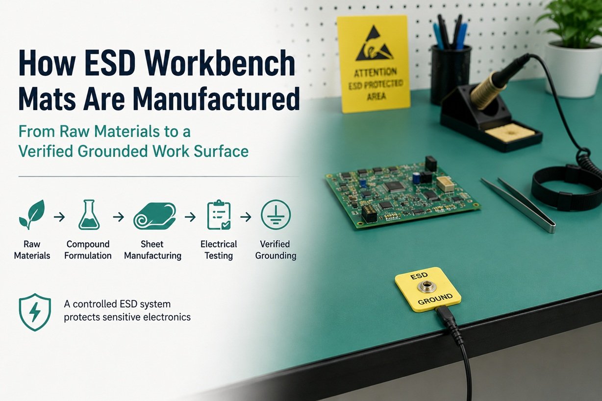
How ESD Workbench Mats Are Made—and Why Manufacturing Quality Matters in PCB Assembly
Modern PCB assembly depends on increasingly small and sensitive electronic components. Engineers carefully control soldering profiles, component placement, inspection, and testing, but the work surface beneath the PCB is also part of the manufacturing environment.
An ESD workbench mat may look like a simple rubber sheet. In reality, its performance depends on material formulation, layer construction, curing, thickness control, electrical resistance, grounding, and quality verification.
The complete engineering chain can be viewed as:
Raw Materials → Compound Formulation → Sheet Manufacturing → Electrical Testing → Workbench Installation → Grounding → Periodic Verification
Understanding this process helps PCB manufacturers evaluate an ESD work surface by measurable properties rather than appearance alone.
Why PCB Assembly Needs a Controlled Work Surface
During PCB assembly, inspection, programming, testing, and repair, sensitive devices can be exposed to electrostatic charge generated by people, tools, packaging, chairs, clothing, and other materials.
The objective of an ESD mat is not simply to make the table conductive.
Instead, the work surface should become part of a controlled electrostatic discharge system.
A typical workstation may include:
ESD Work Surface
↓
Grounding Snap
↓
Ground Cord
↓
Common-Point Ground
↓
Verified Ground Reference
The electrical characteristics of that path begin with how the mat itself is manufactured.
1. Manufacturing Starts With Material Formulation
Rubber ESD mats are normally manufactured from engineered compounds.
Depending on the product design, the formulation may include:
- Base elastomer
- Conductive or dissipative additives
- Fillers
- Curing agents
- Processing aids
- Pigments
- Stabilizers
The engineering challenge is balance.
Adding conductive material does not automatically create a better ESD work surface. The finished material must combine suitable electrical behavior with mechanical characteristics such as flexibility, durability, dimensional stability, wear resistance, and cleanability.
For PCB workstations, the surface must also withstand repeated handling of boards, tools, fixtures, and production materials.
This is why ESD mat performance starts with formulation rather than with the grounding cord installed later.

2. Why Two-Layer Rubber Construction Is Used
Many industrial ESD bench mats use two-layer rubber construction.
A simplified cross-section is:
Upper Working Layer
↓
Lower Layer
↓
Grounding System
The upper layer provides the working surface where PCBs and electronic components are handled.
Depending on the product design, the lower layer can have different electrical characteristics and contribute to the intended path toward the grounding system.
The two layers therefore work as an engineered structure.
This also explains why judging an ESD mat only by color can be misleading. Green, blue, gray, or black does not by itself establish electrical performance.
Resistance must be measured.
3. Mixing Determines Electrical Uniformity
Material preparation is an important manufacturing stage because conductive or dissipative additives should be distributed consistently throughout the compound.
Poor distribution can contribute to variation across the finished sheet.
From a factory quality perspective, the objective should therefore be:
Uniformity across the surface
Consistency across the production roll
Repeatability between production batches
This becomes important when a large mat is cut into multiple workbench sizes.
If electrical characteristics vary significantly across the original material, different workstations could receive pieces with different behavior.
Manufacturing consistency reduces this risk.
4. Sheet Forming and Thickness Control
After mixing, the rubber compound is formed into sheets or rolls.
Thickness is an important production parameter because it influences mechanical durability, flexibility, installation, and long-term wear.
For example, depending on the application and product specification, rubber ESD work surfaces may be produced in thicknesses such as 2 mm or 3 mm.
Factory inspection should not rely on one thickness measurement.
A practical multi-point inspection can include:
- Front left
- Front right
- Center
- Rear left
- Rear right
A digital caliper or suitable thickness gauge can document these values.
For custom PCB workstations, dimensional control also matters because mats may be cut according to specific bench widths, depths, equipment locations, or grounding-point positions.
5. Curing Turns the Compound Into the Finished Work Surface
For rubber mats, curing is another critical production stage.
Temperature, pressure, time, and formulation interact to determine the properties of the finished material.
After curing, manufacturers can inspect for visible problems such as:
- Bubbles
- Delamination
- Surface irregularities
- Edge defects
- Thickness variation
- Contamination
- Physical damage
However, visual inspection only confirms physical appearance.
A mat that looks perfect still requires electrical testing.
This distinction is important in ESD manufacturing:
Visual QC ≠ Electrical QC
Both are required for a meaningful inspection process.
6. Electrical Resistance Testing
Once the material has been produced, electrical measurements can be used to evaluate its performance.
Two important measurements for ESD work surfaces are point-to-point resistance and resistance-to-ground.
Point-to-Point Resistance
PTP evaluates resistance between two positions on the work surface:
Electrode A → Mat Surface → Electrode B
This can help identify whether electrical behavior is reasonably consistent across different areas.
Resistance-to-Ground
RTG evaluates the electrical path from a selected point on the work surface toward the grounding connection:
Electrode → Work Surface → Grounding Connection
The measurements answer different questions.
PTP: How does resistance behave across the surface?
RTG: What is the resistance path toward ground?
The applicable test method, voltage, electrodes, environmental conditions, and acceptance criteria should be defined by the relevant ESD control procedure rather than guessed from a product label.
7. Why Five-Point Testing Is Better Than One Reading
Imagine a large workbench mat is tested only at its center.
The measurement passes.
Does that prove the entire working area has identical electrical behavior?
Not necessarily.
A more informative QC procedure can evaluate several locations:
Point 1: Center
Point 2: Front left
Point 3: Front right
Point 4: Rear center
Point 5: Area farther from the grounding connection
Multiple readings can help identify localized variation, contamination, material inconsistency, or damage.
For production traceability, results can be connected to a product or batch number.
A basic record may contain:
| Parameter | Recorded Data |
|---|---|
| Batch | Product identification |
| Thickness | mm |
| Test Method | PTP / RTG |
| Test Voltage | Recorded |
| Temperature | °C |
| Humidity | %RH |
| Resistance | Ω |
| Test Location | Position |
| Result | According to applicable criteria |
The important principle is simple:
Measure the product rather than assuming its performance.
8. From Factory Mat to PCB Workbench
Factory testing does not complete the ESD control process.
The mat must now become part of the workstation.
A properly integrated ESD workbench mat can be connected through:
Work Surface → Grounding Snap → Ground Cord → Common-Point Ground → Ground

Where personnel grounding is required, another path may exist:
Operator → Wrist Strap → Coil Cord → Common-Point Ground

The manufacturer controls the electrical and mechanical characteristics of the mat.
The workstation designer controls how the mat is installed and integrated with the grounding system.
A good mat installed incorrectly can therefore create a poor workstation.
Likewise, an excellent grounding design cannot correct a work surface whose electrical characteristics are unsuitable or inconsistent.
9. Designing the Complete PCB Workbench
An ESD workstation should not be designed around the mat alone.
A practical PCB assembly bench may include:
- ESD work surface
- Grounding snap
- Ground cord
- Common-point ground
- Wrist-strap connection
- Grounded or ESD-compatible tools
- ESD component bins
- PCB racks
- Appropriate packaging
- Ionization where required
The objective is to create a controlled handling environment around sensitive electronic assemblies.
The position of the mat grounding snap should also be considered during workstation design.
It should provide a practical grounding connection without unnecessarily interfering with the main PCB working area.
For customized workbenches, dimensions, shelf positions, grounding locations, lighting, storage, and equipment placement can therefore be planned together.
10. Factory QC and Workstation Verification Are Not the Same
One important engineering distinction is the difference between factory testing and field verification.
Factory QC answers:
Did the manufactured mat meet its specified production requirements?
Workstation verification asks:
Is the installed ESD control system still functioning as intended?
After installation, the work surface may be exposed to:
- Flux residues
- Dust
- Skin oils
- Cleaning chemicals
- Soldering tools
- Heat
- PCB fixtures
- Mechanical wear
- Adhesives
- Packaging materials
These factors can change over time.
This is why a resistance value measured at the factory should not be treated as a lifetime guarantee of workstation performance.
11. Common Workbench Problems
Even when the original mat is manufactured correctly, several problems can develop after installation.
Incorrect grounding: The mat may be connected to an unsuitable or unverified point.
Damaged ground cord: A broken conductor can interrupt the intended electrical path.
Surface contamination: Flux, oil, dust, or cleaning residue can affect surface behavior.
Localized wear: Repeated tool placement, cutting, heat, or mechanical damage can affect part of the mat.
Operator grounding failure: A work surface can function correctly while the wrist strap system has a separate fault.
Nearby insulators: Plastic packaging or fixtures may retain charge even when the bench itself is grounded.
This is why ESD control should be treated as a system rather than a product.
12. The Factory-to-Workbench Quality Chain
The complete lifecycle can be summarized as:
Material Selection
↓
Compound Mixing
↓
Two-Layer Construction
↓
Forming & Curing
↓
Thickness Inspection
↓
Electrical Resistance Testing
↓
Cutting & Grounding Hardware
↓
Workbench Installation
↓
System Verification
↓
Periodic Maintenance
A failure at one stage can affect the final result.
Good manufacturing cannot compensate for incorrect grounding.
Good grounding cannot correct inconsistent material.
And a correctly manufactured and installed workstation cannot be assumed to remain unchanged forever.
Final Thoughts
For PCB assembly, an ESD workbench mat should not be evaluated simply by its color, thickness, or “anti-static” label.
Its performance starts in manufacturing.
Material formulation, mixing, layer construction, curing, dimensional control, resistance testing, grounding hardware, installation, and periodic verification all contribute to the final ESD control system.
For manufacturers and electronics engineers, the better approach is:
Manufacture → Measure → Install → Ground → Verify → Maintain
When these stages are connected, the workbench mat becomes more than a rubber sheet beneath a PCB.
It becomes a measurable part of the electronics manufacturing process.


